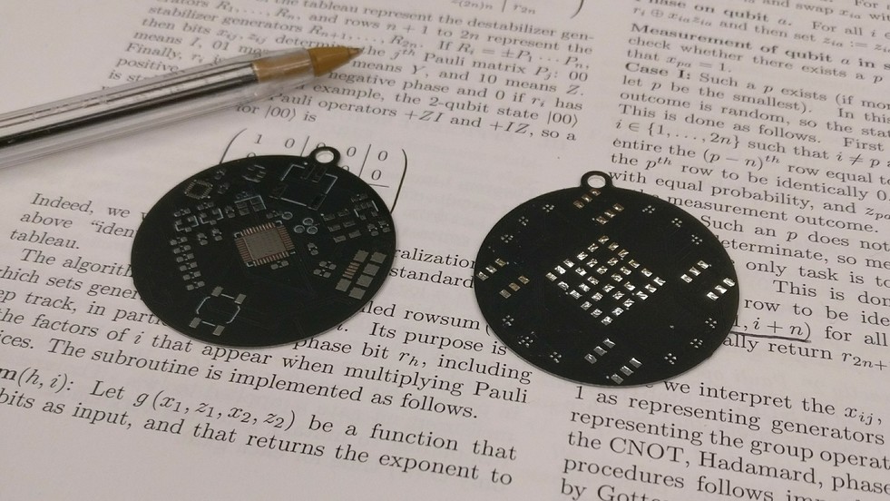
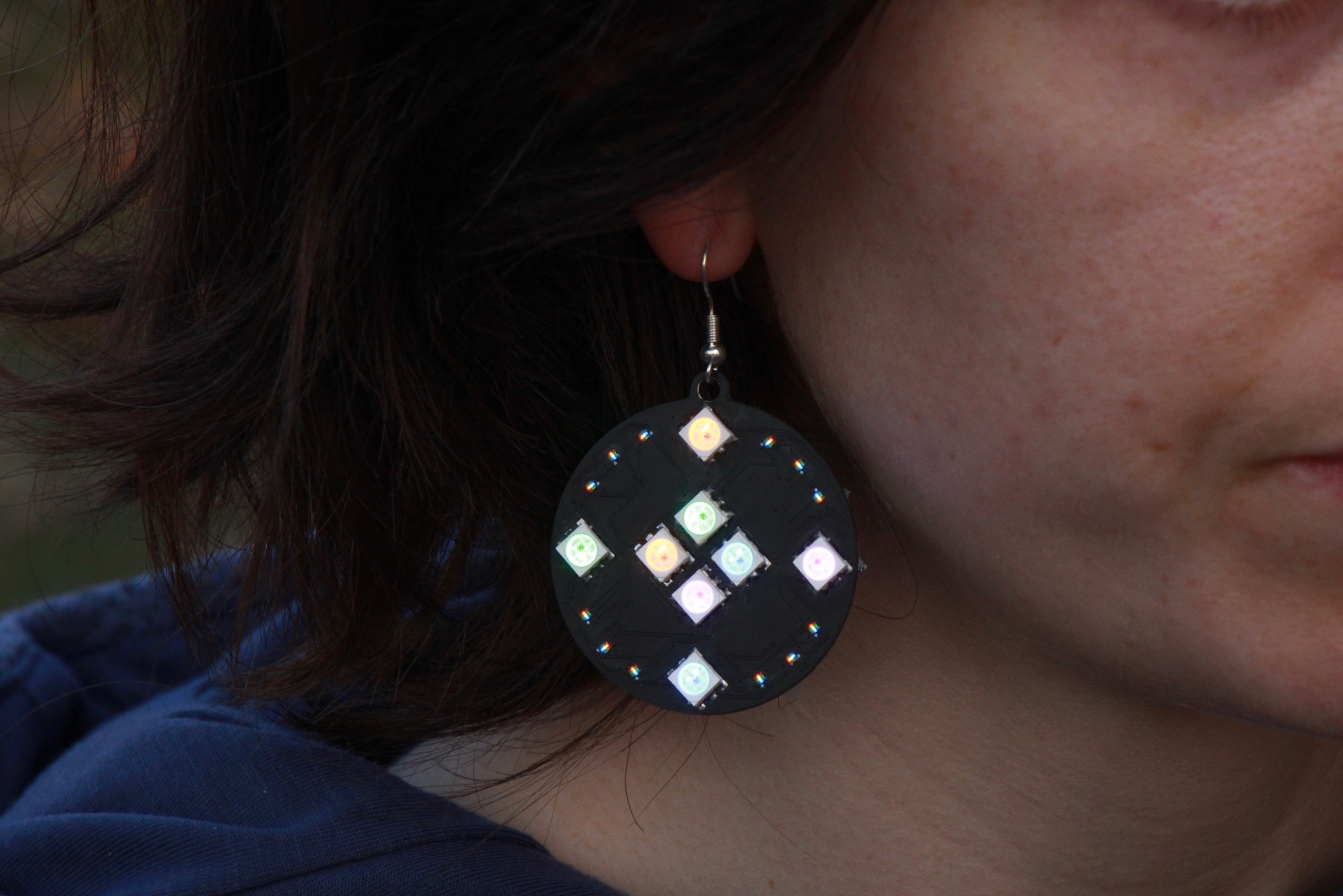
I have been working on a small electronic jewelry-like device meant to teach kids how to program. The device can be seen on the left. As it is an educational project, it certainly needs pleasant teaching materials and visuals. One such visual, meant for the “Engineer’s Diary” where we describe the process of creating the device, is a timelapse of the CAD design for the printed circuit board.
Before we delve into the details of how to produce the timelapse, here is the final result we desire.
The Tools
The Electronics CAD work was done in KiCad, which is an open source tool with
lovely documentation and available tutorials. One of its subtools, pcbnew,
lets you turn the abstract circuit diagram into the actual physical layout of
the device. As with most such tools, the main tasks are to place the required
components judiciously, such that you can route all the electrical connections
between them by drawing traces and puncturing
vias where necessary.
KiCad stores this layout information in a data structure that can be
manipulated with python scripts through the pcbnew python module. This is how
we will create our timelapse - by writing a script that generates an image
frame for each step of the process.
We will also need ImageMagick and Inkscape for some command line image
manipulation, as well as ffmpeg for stitching the final video together.
Loading the PCB (Printed Circuit Board) File and Setting the Plotting Functionality

The layout design, whose physical incarnation you can see on the right, is all stored
in a .pcbnew file. We can open it inside of our timelapse script.
We also need to deal with the much more cumbersome task of setting up the
plotting functionality of KiCad. This is done in a quite imperative style,
where we need to carefully track the global state of the plotter. We create the
pctl object which will control the plotter functionality and the popt
object through which the current plotter settings are updated:
from pcbnew import *
board = LoadBoard("./kits_prettyvis.kicad_pcb")

pctl = PLOT_CONTROLLER(board)
popt = pctl.GetPlotOptions()
popt.SetOutputDirectory("prettyvis")

popt.SetPlotFrameRef(False)
popt.SetLineWidth(FromMM(3.))
...
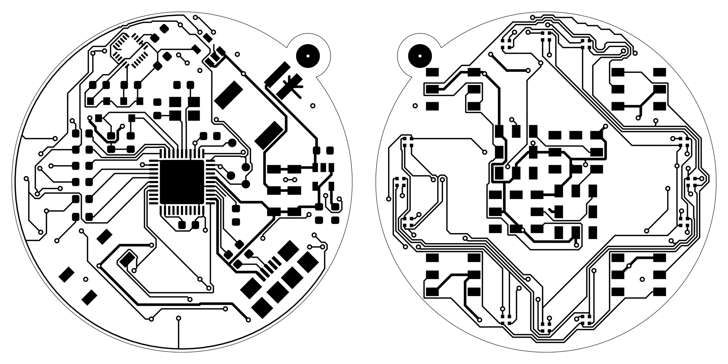
If we just print out the current state of the board by opening a plotting file
pctl.OpenPlotfile(filename, PLOT_FORMAT_SVG, title) followed by pctl.PlotLayer() we will obtain something like this:

Reproducing the Step-by-step Process of Designing the Board
Now all that is left is to delete one-by-one each trace and each component
until we are left with just the outline of the board. Thankfully KiCad stores
traces and components in the order of their modification, which lets us very
naturally loop through them. There are two important lists of entities,
board.GetTracks() which enumerates all the traces and vias, and
board.GetModules() which enumerates the monolithic components like chips and
resistors. One by one we delete each track and then we delete each module. In
between each deletion, we plot the current state of both the front and back of
the board. This gives the illusion of the most recent additions to the board
slowly disappearing.
for i,t in enumerate(board.GetTracks()):
    pctl.SetLayer(F_Cu) # select only the front copper layer for plotting
    popt.SetMirror(False)
    pctl.OpenPlotfile("all_front_track_%05d"%i, PLOT_FORMAT_SVG, "Pretty!")
    pctl.PlotLayer()
    pctl.SetLayer(B_Cu) # select only the back copper layer for plotting
    popt.SetMirror(True)
    pctl.OpenPlotfile("all_back_track_%05d"%i, PLOT_FORMAT_SVG, "Pretty!")
    pctl.PlotLayer()
    t.DeleteStructure() # delete the most recent structure
for i,m in enumerate(board.GetModules()):
    ... # do the same for all monolithic components
Cleanup and Final Touches
The svg files that KiCad produces can be messy and might have confusing bounding boxes. Inkscape can be invoked on the command line to find the appropriate bounding box and export a png file:
for i in range(len(allfiles)):
    os.system("inkscape -z -e prettyvis/front_%05d.png --export-area-drawing --export-dpi=300 prettyvis/front_%05d.svg"%(i,i))
If we want to recolor these black and white images, an inefficient but trivial way is to invoke ImageMagick:
for i in range(len(allfiles)):
    os.system("mogrify -fuzz 30%% -fill purple -opaque black prettyvis/front_%05d.png"%(i))
And we can use the same toolkit to splice the front and back image together:
for i in range(len(allfiles)):
    os.system("montage prettyvis/*_%05d.png[1180x1180] -geometry +40+40 -tile 2x1 prettyvis/mon_%05d.png"%(i,i))
Lastly, we just need to use ffmpeg to splice all these images together into a timelapse video. It would be important to separate the images corresponding to adding tracks from those corresponding to adding components, as the former would need to loop much faster given their much larger quantity. The following two commands ended up being sufficient to turn each set of pictures in a short video. Then one just needs to concatenate the two videos and they have their timelapse.
ffmpeg -y -framerate 15 -pattern_type glob -i "prettyvis/slow/mon*.png" -c:v libx264 -r 30 -pix_fmt yuv420p prettyvis/1.mp4
ffmpeg -y -framerate 250 -pattern_type glob -i "prettyvis/fast/mon*.png" -c:v libx264 -r 30 -pix_fmt yuv420p prettyvis/2.mp4
An IPython notebook that can walk you through this process, together with an example pcb file can be found in the repository of the SpinWearables outreach team. You can find it on github.

If this piqued your interest, please consider supporting our upcoming Kickstarter. The entirety of the money gathered will be used to organize STEM outreach events for kids, teaching them about Computer Science, Electronics, and Physics. You can sign up to be notified when we launch in March. Or follow the project on twitter @SpinWearables.